Lab 4
FPGA
Objective
The goal of this lab is to implement an FPGA module that can detect shapes and colors from the camera input and pass the information to the Arduino.
Procedure
To complete this lab, we split into two teams, Team Arduino and Team FPGA. The parts of the lab that are being implemented are the red blocks in the following diagram.
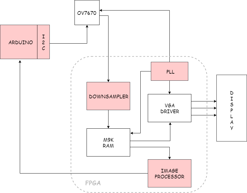
Block Diagram
To begin, both groups set up the PLL. To do this, we set clock inclk0 to 50 MHz, clock c0 to 24 MHz, clock c1 to 25 MHz, and clock c2 to 50 MHz. These clocks all have a duty cycle of 50%. We then went through the DE0_NANO.v file and changed all of the CLOCK_50 to c2 because the other clocks are phase-locked to this clock. After the PLL was set up, we split into the two teams and proceeded as follows.
Team Arduino (Alex and Sid)
Our objectives were to wire the camera, communicate with the Arduino, and read treasure data from the FPGA.
Arduino-Camera communication
First, we looked at the OV7670 Data Sheet to wire the data pins on the camera to the FPGA. Then, we wired up the following circuit to connect the camera to the Arduino.
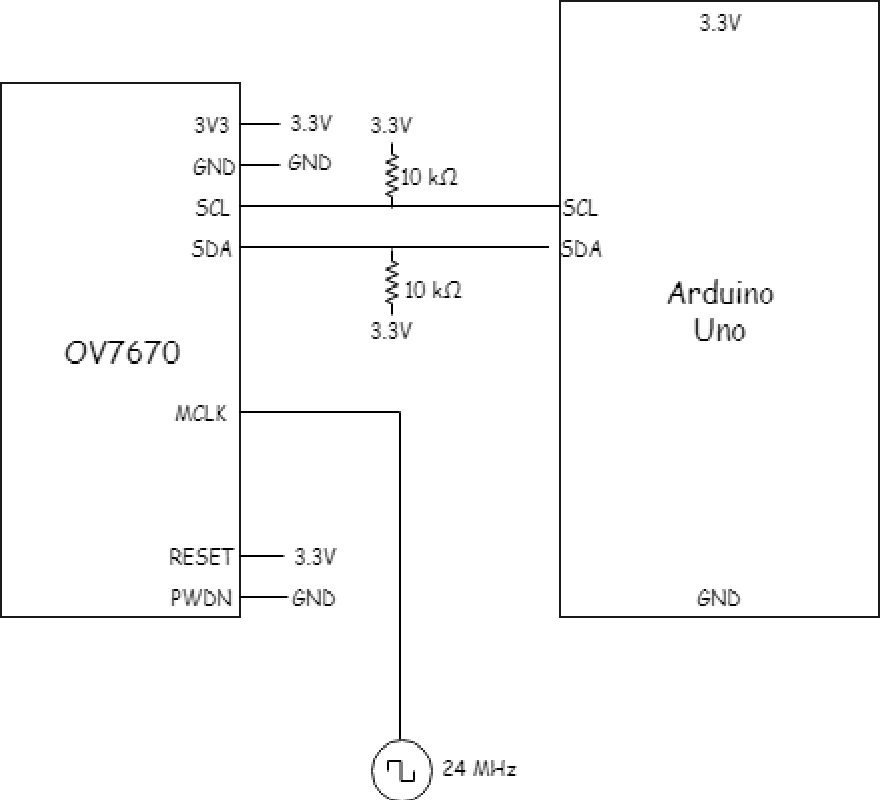
Camera Wiring Diagram from Lab 4 instructions.
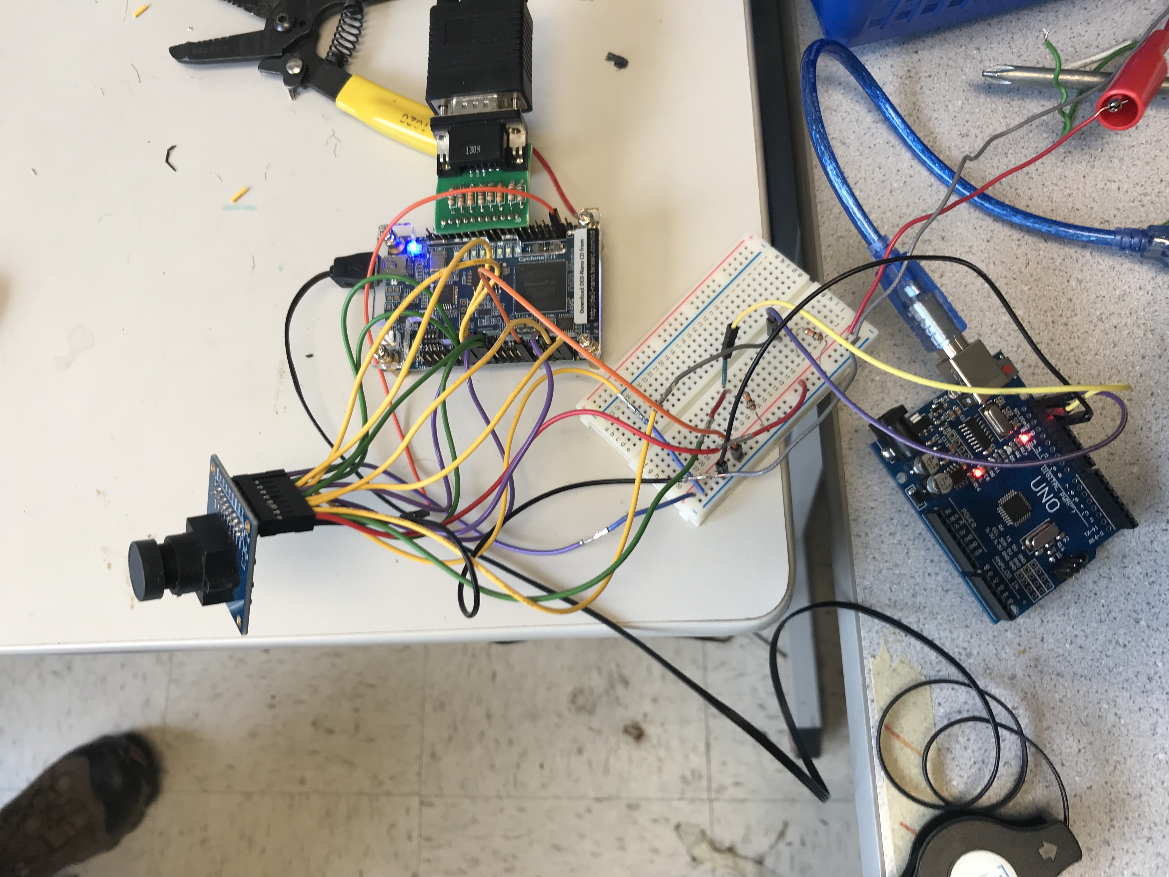
Camera wired to Arduino, according to diagram.
After the camera was wired, we used the OV7670 Data Sheet to determine which registers are responsible for resetting registers, scaling, setting the clock, and changing the output resolution. In the setup function, we read the initial values from the registers using this function:
void read_key_registers(){
  reg11 = read_register_value(0x11); //external clock
  Serial.println( "reg11" );
  Serial.println( reg11 );
  reg12 = read_register_value(0x12); //enable scaling
  Serial.println( "reg12" );
  Serial.println( reg12 );
  reg40 = read_register_value(0x40); //change res
  Serial.println( "reg40" );
  Serial.println( reg40 );
  reg42 = read_register_value(0x42); //change res
  Serial.println( "reg42" );
  Serial.println( reg42 );
  reg0C = read_register_value(0x0C); //change res
  Serial.println( "reg0c" );
  Serial.println( reg0C );
  reg14 = read_register_value(0x14); //change res
  Serial.println( "reg14" );
  Serial.println( reg14 );
  Serial.println( "finished read" );
}
Arduino-FPGA communication
Next, we wrote the appropriate values to the registers based on the data sheet using this function. This code is to show the camera output (to display the color bar test, we used the code in the comments):
 Serial.println("starting write");
  Serial.println(OV7670_write_register( 0x12, 0x80 ));
  //delay
  delay(100);
  Serial.println(OV7670_write_register( 0x12, 0x0C ));  //c should disable test, E should enable everything
  Serial.println(OV7670_write_register( 0x11, 0xC0 ));
  Serial.println(OV7670_write_register( 0x0C, 0x08 ));
  Serial.println(OV7670_write_register( 0x40, 0xD0 ));
  Serial.println(OV7670_write_register( 0x42, 0x00 )); //more color test reg 42, 0 will turn off, 08 will turn on
  Serial.println(OV7670_write_register( 0x14, 0x0B ));
  // to turn color test on:
  // replace "Serial.println(OV7670_write_register( 0x12, 0x0C ));" with  Serial.println(OV7670_write_register( 0x12, 0x0E ));
  // replace "Serial.println(OV7670_write_register( 0x42, 0x00 ));" with Serial.println(OV7670_write_register( 0x42, 0x08 ));
To test, we displayed these values to the serial monitor (on the Arduino) to make sure we were getting the correct value.
Team FPGA (Rebecca and Chloe)
Our task was to modify the DE0_NANO, including the downsampler and the image processor.
First, we calculated the screen width and screen height (from prelab) to be 176 and 144 respectively. We then defined SCREEN_WIDTH to be 176 and SCREEN_HEIGHT to be 144, and also set RED = 8’b11100000, GREEN = 8’b00011100, and BLUE = 8’b00000011 to be used for test patterns. We then set up all of the clocks in the DE0_NANO by creating wires for c0_sig, c1_sig, and c2_sig and hooked these clocks up to the PLL module as follows:
sweetPLL	sweetPLL_inst (
	.inclk0 ( CLOCK_50 ),
	.c0 ( c0_sig ), //24
	.c1 ( c1_sig ), //25
	.c2 ( c2_sig )  //50 - phase synchronized with c0 and c1
	);
Then, we connected the VGA adapter to the FPGA’s GPIO_0[5] through GPIO_0[23] so we could connect the FPGA to the monitor.
Displaying M9K block
Next, we created a buffer reader that connected the M9K RAM to the VGA Driver. To do this, we updated the read address module to add a test pattern. We decided to make a test pattern that had the screen width and height green, with the exception of a line of slope -1 which would be red. Here is our updated read address module:
always @ (VGA_PIXEL_X, VGA_PIXEL_Y) begin
		READ_ADDRESS = (VGA_PIXEL_X + VGA_PIXEL_Y*`SCREEN_WIDTH);
		if(VGA_PIXEL_X==(`SCREEN_WIDTH-1) || VGA_PIXEL_Y==(`SCREEN_HEIGHT-1)) begin
				VGA_READ_MEM_EN = 1'b0;
		end
		else begin
				VGA_READ_MEM_EN = 1'b1;
		end
end
Here is the output of the buffer reader:

Output of Buffer Reader
Camera-FPGA Communication
Next, we created the downsampler module, since the pixel data is 16 bits throughout 2 cycles, and we only need 8 bits. To implement this, we created the registers, cycle. Cycle is a 1 bit value that determines whether it is on the first 8 bits of the pixel data or the second 8 bits of the pixel data.If cycle is low, we set pixel_data_RGB332[1:0] to the most significant bits of blue data, update cycle, and make sure that we are not writing to memory by setting W_EN to 0. If cycle is high, we set pixel_data_RGB332[7:5] to be the most significant bits of red data and pixel_data_RGB332[4:2] to be the most significant bits of green data. We also needed to reset the locations of pixel x when there was a new frame or a new line, and reset the location of pixel y when there was a new frame. To do this, we looked at VSYNC and HREF. We also used an always block at the positive edge of PCLK to check when the next 8 bits of pixel data are taken in.
//downsampler
reg cycle = 1'b0;

always @ (posedge PCLK) begin
	if (VSYNC) begin
		X_ADDR = 0;
		cycle = 0;
		W_EN = 0;
		pixel_data_RGB332[7:0] = 0;
	end
	else begin
		if (!HREF) begin
			X_ADDR = 0;
			cycle = 0;
			W_EN = 0;
			pixel_data_RGB332[7:0] = 0;
		end
		else begin
			if (!cycle ) begin
				cycle = 1'b1;
				W_EN = 0;
				X_ADDR = X_ADDR;
				pixel_data_RGB332[1:0] = {GPIO_1_D[12], GPIO_1_D[11]};
			end
			else begin
				pixel_data_RGB332[7:5] = {GPIO_1_D[15], GPIO_1_D[14], GPIO_1_D[13]};
				pixel_data_RGB332[4:2] = {GPIO_1_D[10], GPIO_1_D[9], GPIO_1_D[8]};
				cycle = 1'b0;
				W_EN = 1;
				X_ADDR = X_ADDR + 1'b1;
			end
		end
	end
end
Next, we implemented the image processing module. To do this, we used an always block at the posedge of c1_sig and the negedge of VGA_VSYNC_NEG. We created registers to count the blue and red pixels and temporary registers for blue count and red count. If VGA_VSYNC_NEG is low, this means there is a new frame, so we want to compare the values in the registers, and if blue is higher than red and above a certain threshold, we set the result to be 2’10 to represent blue. If red was higher than blue and above a certain threshold, then we set the result to be 2’b01. If neither of these cases were true, meaning no color is detected, we set result to 2’b00. Then, if VGA_VSYNC_NEG is high, we take the data from pixel_data_RGB332 and increment either red count or blue count.
always @ (posedge CLK, negedge VGA_VSYNC_NEG) begin
		if (!VGA_VSYNC_NEG) begin
			if (BLUECOUNTTEMP > REDCOUNTTEMP && BLUECOUNT > 10'b0001100100) begin
				RESULT = 2'b10; //when color is 10, blue
			end
			else if (REDCOUNTTEMP > BLUECOUNTTEMP && REDCOUNT > 10'b0001100100) begin
				RESULT = 2'b01; //when color is 01, red
			end
			else begin
				RESULT = 2'b00; //no color detected
			end
			BLUECOUNT = 0;
			REDCOUNT = 0;
		end
		else begin
			if (PIXEL_IN[7:6] > PIXEL_IN[1:0] && PIXEL_IN[7:6] > PIXEL_IN[4:3]) begin
				REDCOUNT = REDCOUNT + 1'b1;
			end
			else if (PIXEL_IN[1:0] > PIXEL_IN[7:6] && PIXEL_IN[1:0] > PIXEL_IN[4:3]) begin
				BLUECOUNT = BLUECOUNT + 1'b1;
			end
			REDCOUNTTEMP = REDCOUNT;
			BLUECOUNTTEMP = BLUECOUNT;
		end
end
Later, we will update the image processing modules so that we can detect what shapes the treasures are.
Integration
After both teams were completed with their tasks, we began to put the two segments together. We took the data from the OV7670, and saved it to memory using the FPGA team’s downsampler. The camera team set the registers to output a color bar test. To connect the Arduino to the FPGA, we connected 2 output pins (GPIO_0_D[31] and GPIO_0_D[31])from the FPGA and inputted them to the Arduino (pins 8 and 9). These got the results from the image processor. This is the code we used to set the output on the FPGA pins:
assign GPIO_0_D[31] = RESULT[1];
assign GPIO_0_D[33] = RESULT[0];
assign GPIO_0_D[29] = 1'b1;
These were used as inputs to the Arduino:
pinMode(8, INPUT);
pinMode(9, INPUT);
After debugging both the registers from Team Arduino and the downsampler from Team FPGA, we got the following output:

Output of Color Bar Test
Next, we toggled off the registers that enabled the color bar test. We got a clear image from the camera, and it was easy to distinguish between the red treasures and the blue treasures. Here is a video of the camera:
We then debugged our image processing code. To tell if our image processor was working correctly, we output “RED”, “BLUE”, or “NO COLOR” to the serial monitor.
Demonstration: